Shandong Good Achievement | Device production cost reduced by more than 50%, 12 inch lithium niobate crystal opens up a new era of optoelectronics
Research has shown that the world's leading microwave photonic chip developed based on lithium niobate optical platform can use photons for ultrafast analog electronic signal processing and computation, which is 1000 times faster than traditional electronic processors. It not only has lower energy consumption, but also has a wide range of applications, covering multiple fields such as wireless communication, high-resolution radar, artificial intelligence, computer vision, image/video processing, etc.
Nowadays, it is referred to as'; Industrial Seed Materials; The lithium niobate crystal is undergoing a disruptive transformation in the optoelectronic industry. In May 2024, Shandong Hengyuan Semiconductor Technology Co., Ltd. collaborated with research teams from Shandong University and Jinan University to successfully independently develop a 12 inch (300mm diameter) optical grade lithium niobate crystal. It is reported that after two years of research and development, and experiencing dozens of failures, the R&D team has successively overcome the key core technologies of the entire chain, including the design of 12 inch lithium niobate crystal production equipment, crystal growth and defect control, and crystal post-processing. Finally, they have broken through the growth technology of 12 inch lithium niobate crystals first in the world, marking a significant breakthrough in the development level of key materials in China's optoelectronic industry.
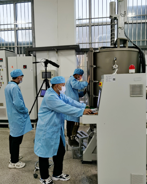
After experiencing dozens of failures, the R&D team first broke through the 12 inch lithium niobate crystal growth technology globally
New breakthrough in lithium niobate crystal technology from 6 inches to 12 inches
Lithium niobate crystals have become the core foundational material driving the development of integrated photonics technology due to their outstanding piezoelectric, electro-optic, acousto-optic, and nonlinear optical properties. This material has a wide range of applications in cutting-edge fields such as high-performance filters, electro-optical devices, holographic storage, 3D holographic displays, nonlinear optical devices, and optical quantum communication, providing strategic foundational support for the development of integrated photonics.
Previously, Hengyuan Semiconductor has successfully achieved mass production of 6 to 8-inch Z-axis and X-axis optical grade lithium niobate crystals through technological transformation. However, the global market for large-sized optical grade lithium niobate crystals has long been monopolized by foreign companies, with over 90% of the market share held by foreign companies and export restrictions imposed on related products. The mainstream technology in this field in China is still dominated by 6-inch crystals, and there is an urgent need for technological upgrading.
With the rapid development of high-performance optoelectronic chip technology, the demand for large-sized lithium niobate crystals ranging from 8 to 12 inches is becoming increasingly urgent. Hengyuan Semiconductor collaborated with a research team led by Professor Liu Hong from Shandong University and Professor Sun Dehui from Jinan University to propose and overcome the growth technology of 12 inch lithium niobate crystals for the first time.
The research team has made breakthroughs in key technologies such as crystal production equipment design, crystal growth process, and defect control. They have taken the lead in achieving batch production technology for 8-inch crystals in China and successfully developed the world's first 12 inch ultra large optical grade lithium niobate crystal.
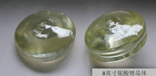
8-inch (200mm diameter) lithium niobate crystal
Continuously increasing the integration of optoelectronic chips, breaking through the 'post Moore era'
The industry generally believes that integrated optoelectronic technology based on lithium niobate crystals is as disruptive as silicon-based integrated circuit technology back then, so lithium niobate is also known as "optical silicon". From the perspective of the technological potential of "optical silicon", there is a well-known rule of thumb in the semiconductor industry, known as "Moore's Law": the number of transistors that can be accommodated on an integrated circuit doubles approximately every 18 to 24 months, driving processor performance to double every two years while reducing prices by half.
Moore's Law to some extent reflects the speed of information technology development, including rapid performance improvements and significant cost reductions. However, with the accelerated development of emerging technologies such as the Internet of Things, artificial intelligence, and autonomous driving, there is an increasing demand for data transmission speed, storage density, and computing power. This has led to a sustained growth in the market demand for high-performance, low-power, and cost-effective chips. This trend not only drives continuous innovation in chip technology, but also poses new challenges for the future development of the semiconductor industry.
In today's exponential rise in demand for IoT and AI computing power, integrated circuit chips based on electronic and silicon materials have approached the physical ceiling, and the development of information technology has entered the "post Moore era". As a result, scientists have shifted their focus to photon chips that are faster, consume less energy, and have more stable performance.
Integrated optoelectronic chips use photons for ultrafast analog electronic signal processing and computation, without being limited by program size, making them 1000 times faster than traditional electronic processors. It is precisely because of the continuous development of integrated optoelectronic technology that Moore's Law is expected to continue.
The lithium niobate crystal produced by Hengyuan Optoelectronics is the upstream raw material for integrated optoelectronic chips. Compared to 8-inch lithium niobate crystals, 12 inch lithium niobate crystals can increase the integration of optoelectronic chips by 2-3 times and reduce device production costs by more than 50%.
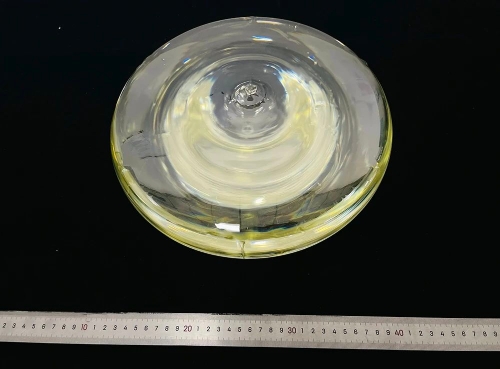
12 inch oversized lithium niobate crystal
The successful application of large-sized lithium niobate crystals promotes the localization of optical grade lithium niobate crystals
It is understood that the R&D team has mastered the key core technologies of the entire chain, including equipment design, uniform polycrystalline material preparation, crystal growth and defect control, and crystal post-treatment. Within the China Europe Manufacturing International Port located on Aerospace Avenue in Jinan High tech Zone, 12 inch lithium niobate crystals are currently being produced.
In the dust-free workshop of Hengyuan Optoelectronics, 8 crystal growth furnaces are arranged in sequence. The person in charge of Hengyuan Semiconductor explained that the raw materials for these crystals are high-purity niobium oxide and lithium carbonate. After mixing, pressing, and sintering, the raw materials are placed in a crystal growth furnace and grown using the pulling method. After about ten days, they will grow into a standard cylinder. After annealing and polarization, the cylinder is cut into rough wafers, chamfered, ground, polished, and cleaned, resulting in lithium niobate wafers. The successful development of 12 inch lithium niobate crystals has further propelled Jinan on the path of integrated optoelectronic industry development.
At present, the large-sized lithium niobate crystals developed by Hengyuan Semiconductor have been successfully applied in products such as Jinan Crystal Positron Single Crystal Thin Film, gradually replacing imported products from Japan and helping to promote the localization process of optical grade lithium niobate crystals. The person in charge of Hengyuan Semiconductor stated that the larger the crystal size, the lower the cost per unit chip, which is the foundation of the industrialization of photonic chips. Within three years, Hengyuan Semiconductor plans to achieve an annual wafer production of 250000 pieces. With the further promotion and application of this achievement, the economic benefits will exceed 100 million yuan in the future, which will help the rapid development of China's optoelectronic basic raw materials and effectively ensure the independent and controllable development of the optoelectronic industry chain.
Information source: Shandong Provincial Department of Science and Technology (official website)